MSc thesis project proposal
Fabricating high-resolution flip-chip interconnects by step & stenc
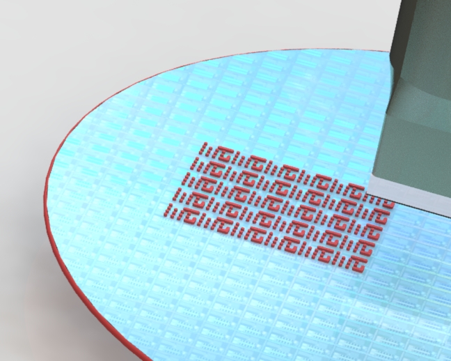
One of the key technologies in assembly and packaging is flip-chip interconnect, where chips are connected face-to-face with solder balls or solder-copper pillars as an electrical and mechanical interconnect. Alternatively a flip-chip interconnect could also be made with conductive epoxy or novel materials, such as nanometallic paste. Such materials can be patterned through stencil printing, but unfortunately this technology is limited to feature sizes of about 30 um. A novel approach to enable further downscaling of flip-chip interconnect is to develop a new high-resolution stencil print technology. Key in this project is to use a combination of MEMS techniques to make a small stencil mask and pick-&-place assembly tools to stepwise apply this mask over larger areas.
Assignment
Design and manufacturing
- Learn the relevant MEMS fabrication techniques and cleanroom lab skills.
- Design stencil mask with test patterns for selected conductive epoxies and nano metallic pastes, including resolution tests and electrical test patterns for further evaluation of the micro stencil process.
- Design a process flow for manufacturing the MEMS chips.
- Fabricate the MEMS chips in the EKL cleanroom.
Process development
- Learn to operate the ECTM pick&place machine.
- Learn to operate advanced microscopy for optical inspection and measurement of stencil printed patterns in various stages of the process.
- Learn to operate electrical parameter analysers for automated measurement of the electrical performance.
- Learn to process selected conductive epoxies and nano metallic pastes to fabricate electrical conductive structures.
- Set up a design of experiments (DOE) for stencil printing.
- Define criteria for evaluating the DOE.
- Execute and evaluate the DOE.
Daily supervisor: Ahmed Abdelwahab
Requirements
You are an ambitious hands-on master student from microelectronic or mechanical engineering, materials science or (applied) physics. You have good communication skills in English, you are independent and also a team player. The graduation project will have a total duration of 9 to 12 months (45 to 60 ECTS).
Dissemination
Apart from the regular ECTM progress meetings, mandatory thesis report and presentation, the student is encouraged to publish results in national or international magazines or conferences.
If you are eager to work in a motivating atmosphere with highly skilled colleagues, then contact us!
Contact
dr. Massimo Mastrangeli
Electronic Components, Technology and Materials Group
Department of Microelectronics
Last modified: 2023-07-28